application
Semiconductor: Dicing of various types of package(BGA/QFN/DFN), wafer sawing and grinding.
Optoelectronic: Slotting, dicing and pickling of coated glass and ordinary glass.
Others: Process in which work piece should be covered when machining and uncovered after that without adhesive residue.
Property
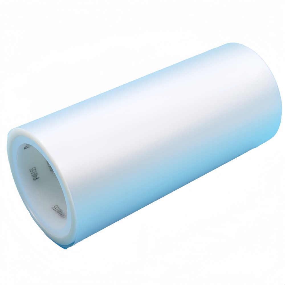
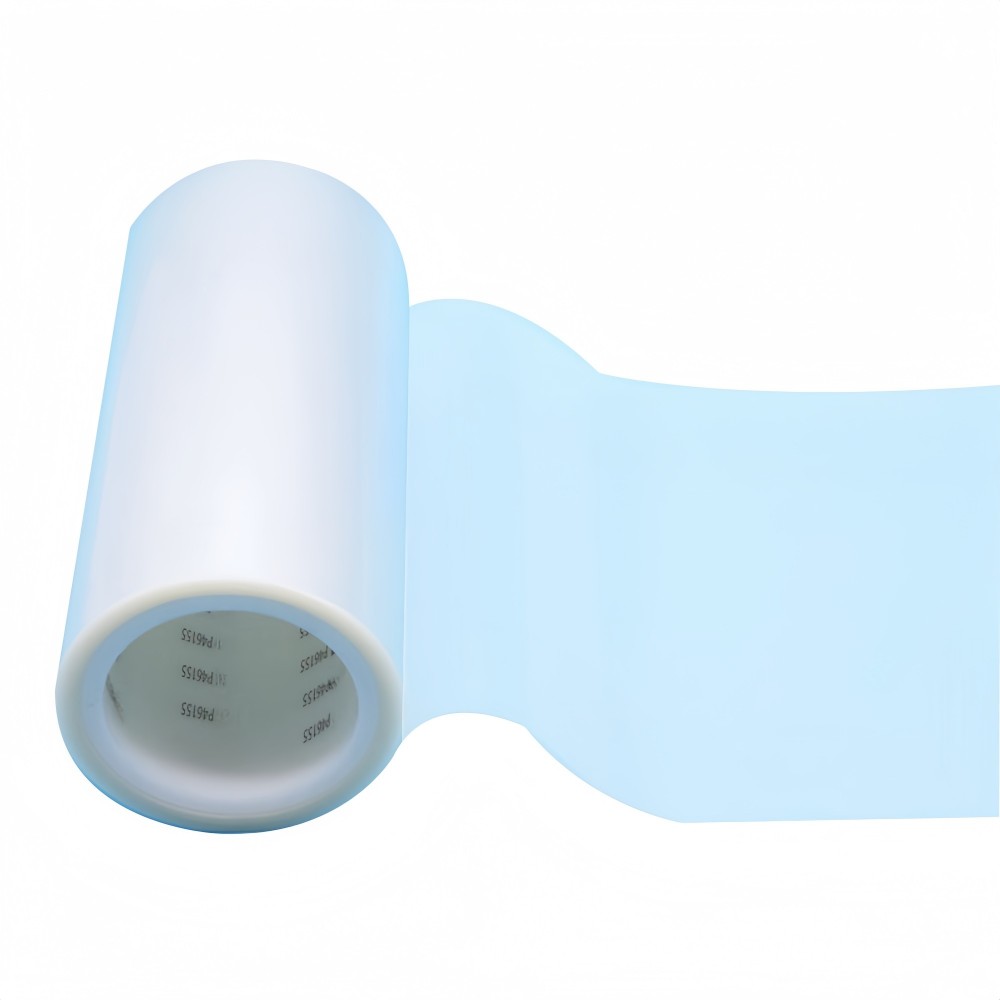
| Property | |||||
| Product Code Technical Parameters | P4640 | P4611 | P4662 | P4616 | P4618 |
| Color | Translucence | Translucence | Translucence | Translucence | Translucence |
| Total Thickness[mm] | 0.08 | 0.11 | 0.155 | 0.16 | 0.16 |
| Backing Thickness[mm] | 0.05 | 0.1 | 0.14 | 0.14 | 0.14 |
| Backing | PET | PET | PO | PO | PO |
| Adhesive | Acrylic | Acrylic | Acrylic | Acrylic | Acrylic |
| 180°Peel Strength (Before UV )[N/inch] | 20 | 8 | 12 | 10 | 20 |
| 180°Peel Strength (After UV )[N/inch] | 0.05~0.1 | 0.03~0.06 | 0.15~0.25 | 0.3~0.5 | 0.05~0.1 |
| UV Exposure Rate[mJ/cm2] | 300~500mJ | 300~500mJ | 300~500mJ | 300~500mJ | 300~500mJ |
| Application | Glass | Glass | MEMS CHIPS | Ceramics | wafer |
description
Features
Adjustable viscosity: When not exposed to ultraviolet light, it has high viscosity and can firmly fix the materials to be cut, such as chips, wafers, etc., to ensure that there is no displacement during the cutting process. After ultraviolet light exposure, the viscosity will decrease rapidly, which is convenient for separating the film from the cut product after cutting is completed, and no residual glue will be left on the surface of the product.
Good flexibility: It can fit well with materials to be cut of various shapes and surfaces, even objects with complex curved surfaces or uneven surfaces, and can be tightly attached to provide a stable fixing effect. At the same time, it can withstand a certain degree of stretching and deformation without breaking during the cutting process.
High transparency: It has a high transmittance for ultraviolet and visible light, which is convenient for optical observation and positioning during the cutting process, ensuring the precision and accuracy of cutting, especially in the field of semiconductor manufacturing where the cutting precision is extremely high. This feature is very important.
Good temperature resistance: It can maintain stable performance within a certain temperature range. During the cutting process, even if a certain amount of heat is generated due to friction and other reasons, the viscosity will not change, the film material will not be deformed or damaged due to the increase in temperature. The tolerable temperature range is generally around -20℃ to 150℃.
Strong chemical stability: It has excellent chemical stability and is not easy to react chemically with the material to be cut and the chemical reagents used in the cutting process, avoiding contamination or corrosion on the surface of the material, ensuring that the quality and performance of the product after cutting are not affected.
High cleanliness: It has low impurity content and particle size, and will not release dust, impurities and other pollutants to the surface of the material during the cutting process, meeting the needs of semiconductor, optics and other industries with extremely high cleanliness requirements.
Application field
Semiconductor industry: In the wafer cutting process, it is used to fix the wafer to ensure the stability of the wafer during the cutting process, prevent the chip from breaking the edge and falling off during cutting, and improve the yield rate of cutting. It can also be used in the chip packaging process, and play a temporary fixing and protection role in the connection process between the chip and the packaging substrate to ensure the smooth progress of the packaging process.
Optical field: In the cutting and processing of optical glass, crystal and other materials, the material can be firmly fixed on the cutting equipment to ensure the cutting accuracy and surface quality, which helps to produce high-quality optical lenses, prisms and other components. For the cutting of optical films, it can provide good support and fixation to prevent the film from wrinkling or shifting during the cutting process, ensuring that the performance and optical properties of the optical film are not affected.
Electronic material processing: In the cutting process of electronic materials such as ceramic substrates and printed circuit boards (PCBs), UV Dicing Film can fix these materials on the cutting table, which is convenient for high-precision cutting and processing, meeting the development needs of miniaturization and high density of electronic components. For the cutting of flexible electronic materials such as flexible circuit boards (FPCs) and organic films, it can adapt to the soft characteristics of the materials, provide stable fixation, and achieve fine cutting.
Other fields: In the manufacture of micro-electromechanical systems (MEMS), it is used to fix tiny mechanical structures and chips, which is convenient for cutting, packaging and other processes to ensure the performance and reliability of MEMS devices. In the jewelry processing industry, it can play a fixing role when cutting materials such as gemstones and jade, which helps to achieve precise cutting, reduce material loss, and improve the quality and efficiency of jewelry processing.